PCF8591 is A single power supply. Low power consumption type 8 COMS A/D.D/A conversion chip, it has 4 road analog to loseInto the channel. All the analog output channel and one I2C bus interface. The device I2C address from low three by the corePiece of A0, A1 and A2 three address pins decision, so the same under the condition of without increasing any hardware I2C totalLine up to eight of the same type can be connected device. The device has a multi-channel analog input. On track. 8 bits A/D conversion and 8 bit D/A conversion, etc. A/D and D/A transfer of the maximum conversion rate of the I2C busLose rate decision.
PCF8591 has the following features:
1. The single power supply;
2. Normal working voltage range of 2.5 V to 6 V.
3. Through the I2C bus to complete data input/output;
4. The device address by three pins decision;
5. The sampling frequency is determined by the I2C bus transmission rate;
6.4 way for analog input programmable input single-ended or differential input;
7. Can be configured automatic conversion channel number increase function;
8. Analog voltage range for VSS to VDD;
9. On track keeping function;
10.8 A successive approximation A/D conversion;
11. All the way with analog output the multiplication of D/A conversion.
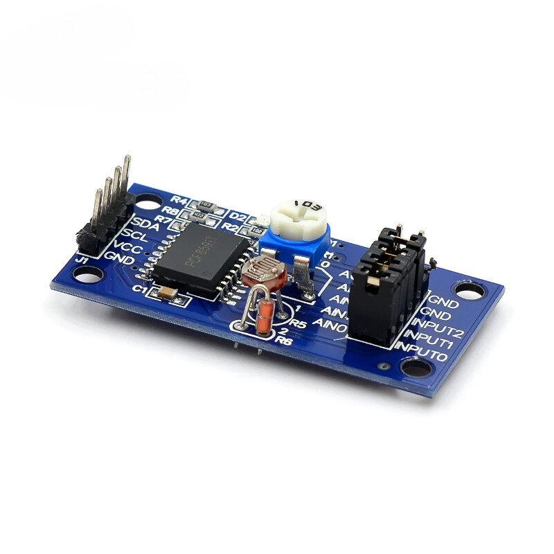
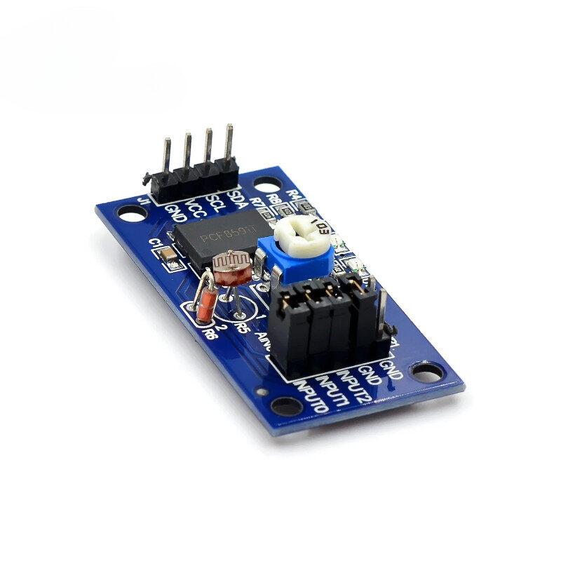
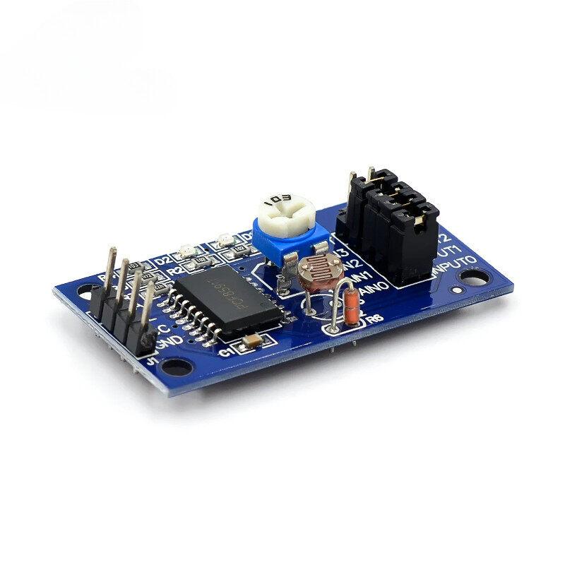
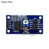
Module description:
1. The module used in chip for PCF8591T, patch encapsulation
2. Support four-way analog voltage acquisition signal input (voltage input range 0-5 v)
3. With the power supply module 1 (D1)
4. With DA output module 1 (D2), when DA output voltage reaches a certain value, the indicator, the voltageThe higher the value, the brighter the light
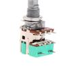
5. 1 0-5 v voltage input module integration acquisition (by blue and white potentiometer to adjust the input voltage)
6. The module integrated 1 road photosensitive resistance (model: 5537), can pass AD collection environmental light intensity
7. The module integrated 1 road thermistor (model: MF58), can pass AD acquisition environment temperature
Connection details:
1. The left 4 row needle:
SDA IIC interface data the (P2.0) microcontroller IO port
SCL IIC interface clock the (P2.1) microcontroller IO port
Positive external 3.3/5 v VCC power supply the anode interface
GND power external 3.3/5 v power cathode cathode interface
2. 8 row needle on the right:
Produce AOUT module DA output port
AIN3 3 analog input signal interface
2 AIN2 analog input signal interface
AIN1 interface 1 analog input signal
0 AIN0 analog input signal interface
3 INPUT3 analog input signal interface
INPUT2 is connected to the thermistor signal input port
INPUT1 is connected to the photosensitive resistance signal input port
INPUT0 is connected to the potentiometer signal input port
3. The jumper cap directions for use:
AIN0 connected with INPUT0 jumper cap, choose potentiometer 0-5 v adjustable voltage access circuit
AIN1 connected with INPUT1 jumper cap, selecting photosensitive resistor connected to the circuit
AIN2 connected with INPUT2 jumper cap, choose thermistor connected to the circuit
Need external analog signal input, please disconnect the jumper cap, the analog signal access AIN0 - AIN3